
What is the AI-Powered Device Modeling?
AI-Powered Device Modeling is the application of artificial intelligence (AI) and machine learning (ML) to create, optimize, and analyze the complex models that predict the behavior of semiconductor devices.
In modern electronics, the physical and electrical characteristics of transistors, memory cells, and other components are incredibly complex. Traditional modeling relies on physics-based equations and massive, time-consuming simulations (like Monte Carlo analysis) [4, 7]. AI-powered modeling uses ML algorithms to learn from vast amounts of simulation or measured silicon data. This allows it to create highly accurate predictive models that are thousands or even millions of times faster to execute, enabling engineers to analyze and optimize designs in ways that were previously computationally impossible [1, 4].
Key Features
- Automation: AI automates highly complex, repetitive, and time-consuming tasks like parameter extraction, layout optimization, and reliability analysis [1, 5].
- Speed: It replaces brute-force simulation methods with rapid, ML-based inference. This can reduce analysis times from weeks or months to just hours or minutes [4, 7].
- High-Dimensional Analysis: AI models can easily handle the interdependencies between thousands of variables (e.g., process variations, temperature, voltage, and layout effects), a task that is extremely difficult for human engineers [7].
- Predictive Power: AI excels at predictive analysis. It can forecast manufacturing yield, device reliability, and performance variations before a chip is fabricated, saving millions in manufacturing costs [3, 4].
Pros and Cons
Pros
- Massively Reduced Time-to-Market: By automating and accelerating design, verification, and modeling, AI significantly shortens the entire chip development cycle [1].
- Improved PPA (Power, Performance, and Area): AI-driven tools can explore a vast design space to find novel and optimal chip layouts that a human might never discover, leading to better-performing, more efficient, and smaller chips [1].
- Higher Yield and Reliability: By accurately modeling rare manufacturing defects and predicting failures, AI helps design more robust circuits that have a higher manufacturing success rate [4, 6].
- Captures “Unknowns”: ML models can learn subtle, complex behaviors and correlations from real silicon data that are not captured by standard physics-based compact models.
Cons
- Data Dependency: AI models are only as good as the data they are trained on. They require massive, high-quality datasets from either simulations (which can be expensive to generate) or physical wafer measurements.
- “Black Box” Problem: A deep learning model might provide a highly accurate prediction (e.g., “this design will fail”), but it can be difficult for engineers to understand why the model reached that conclusion.
- High Initial Cost: Implementing AI-powered workflows requires significant investment in specialized software tools, high-performance computing infrastructure, and engineers with expertise in both AI and semiconductor physics.
- Learning Curve: Adopting these new tools and methodologies requires a shift in thinking and significant training for design teams [2].
Examples of AI-Powered Device Modeling
Here are several key applications in modern semiconductor design:
- SRAM Bit-Cell Yield Modeling
- Key Idea: Modern SRAM (Static RAM) bit-cells are so small (e.g., in sub-5nm nodes) that minuscule, random variations in manufacturing can cause a cell to fail. Calculating the probability of these rare failures (e.g., a “one-in-a-billion” event) would require a computationally impossible number of traditional Monte Carlo simulations. AI-powered tools use a technique called High-Sigma Variation Analysis to intelligently learn the behavior of the circuit and predict this rare failure probability with SPICE-level accuracy in a tiny fraction of the time [4].
- Variability-Aware Circuit Design
- Key Idea: This involves using AI to design circuits that are inherently resilient to manufacturing variations. Instead of just optimizing for a single “typical” case, generative AI algorithms can automatically explore millions of layout and transistor-sizing options. The AI learns which designs are most robust against variations in voltage, temperature, and manufacturing, leading to a final design that has better performance and yield across all possible conditions [5].
- Reliability Modeling
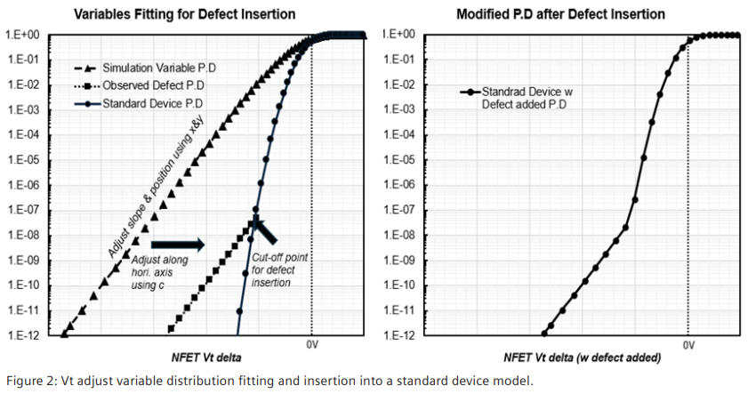
- Key Idea: AI is used to perform predictive failure analysis for a device over its lifetime. By training on data from stress tests (e.g., high-voltage or high-temperature operation), ML models can accurately predict component aging and failure mechanisms, such as equipment breakdowns in the fabrication plant (predictive maintenance) or microscopic defects on a wafer [6]. This allows engineers to forecast the lifespan of a chip under real-world operating conditions.
- Compact Model Parameter Extraction
- Key Idea: A “compact model” is a set of equations that describes a transistor’s behavior, and its “parameters” must be tuned to match real-world measurements. Traditionally, this is a slow, manual, and error-prone process. AI-powered tools use derivative-free optimization (a machine learning technique) to automatically and simultaneously extract tens or even hundreds of parameters. The AI’s goal is to find the best set of parameters that makes the model’s output perfectly fit the measured data, a process it completes dramatically faster and more accurately than a human expert [7].
References
[1] Synopsys. (n.d.). What is AI Chip Design? – How it Works. Retrieved from https://www.synopsys.com/glossary/what-is-ai-chip-design.html
[2] MPE Electronics. (2024, February 27). Benefits & Challenges Of Using AI in PCB Design and assembly. Retrieved from https://www.mpe-electronics.co.uk/2024/02/27/benefits-challenges-of-using-ai-in-pcb-design-and-assembly
[3] PatentPC. (2025, October 3). The Role of AI in Semiconductor Design: How AI Is Optimizing Chip Efficiency (New Data). Retrieved from https://patentpc.com/blog/the-role-of-ai-in-semiconductor-design-how-ai-is-optimizing-chip-efficiency-new-data
[4] Siemens Digital Industries Software. (2025, January 10). Enhancing SRAM Yield Prediction with Solido’s AI-Powered Technologies. Retrieved from https://blogs.sw.siemens.com/cicv/2025/01/10/enhancing-sram-yield-prediction-with-solidos-ai-powered-technologies/
[5] SPIE Digital Library. (2024, December 11). AI-based automated circuit design optimization technology. Retrieved from https://www.spiedigitallibrary.org/conference-proceedings-of-spie/13445/134451A/AI-based-automated-circuit-design-optimization-technology/10.1117/12.3052159.full
[6] IEEE Innovation at Work. (2025, August 7). Revolutionizing Semiconductors Through AI-Driven Innovation. Retrieved from https://innovationatwork.ieee.org/revolutionizing-semiconductors-through-ai-driven-innovation/
[7] Keysight. (2025, September 26). From Equations to Intelligence: Integrating a Machine Learning Optimizer into Compact Model Extraction. Retrieved from https://www.keysight.com/blogs/en/tech/sim-des/eda/dev-mod/from-equations-to-intelligence