
Semiconductor | AI-powered | SRAM | Yield
A full variability-yield analysis workflow, including yield curve prediction and PVT corner exploration with AI
Summary of the demo
- Synthetic SPICE/TCAD-style dataset
- Features: ΔVtn, ΔVtp (mV), ΔL (nm), Vdd (V), Temperature (°C).
- Target: Read SNM (mV).
- N = 5,000 training samples with a simple physics-inspired target + noise.
- Train surrogate models
- Mean predictor: GradientBoostingRegressor (GBR).
- Uncertainty (approx): two GBRs using quantile loss (α=0.05 and α=0.95) to estimate lower/upper prediction quantiles.
- Yield curve estimation
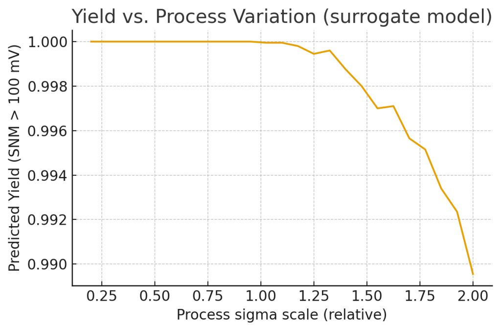
- For a SNM pass threshold (example: 100 mV), the code samples many variation points with varying global sigma scale and evaluates predicted yield = fraction(SNM > threshold).
- This replaces brute-force SPICE Monte Carlo with a fast surrogate.
- PVT corner exploration
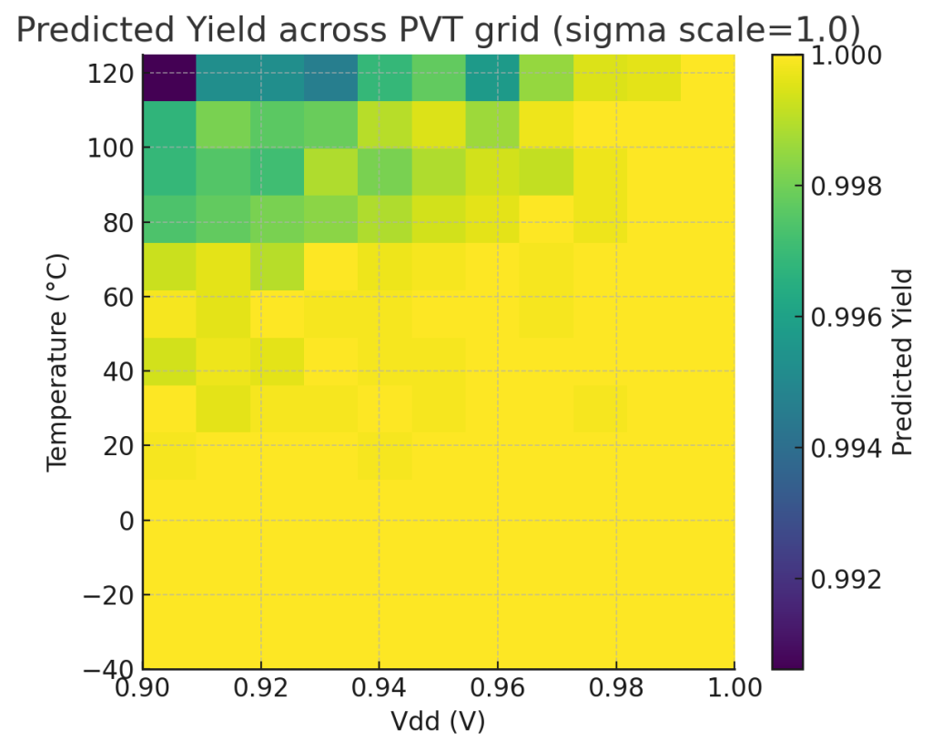
- Grid of Vdd (0.90–1.00 V) and T (−40–125 °C).
- For each corner, the surrogate predicts SNM distribution (by sampling process variations) and computes yield.
- Outputs produced
- Yield vs. process sigma plot (shows predicted yield drop as variation increases).
- PVT heatmap with predicted yield across Vdd/Temp grid.
- Small table showing model MAE (~7.35 mV in the demo) and R² (~0.905), plus sample predictions with 5–95% quantile bounds.
Why this approach works
- Speed: A trained surrogate predicts millions of samples in seconds vs. SPICE which may take hours/days.
- Coverage: You can explore larger parameter spaces (sigma scaling, PVT grids, layout variations) cheaply.
- Actionable yield estimates: Use predicted distributions to compute yield, sensitivity, and identify hotspots.
- Design feedback loop: Feed the ML model’s sensitivity results back to process or layout teams for targeted improvement.
Practical production workflow
- Data collection
- Gather TCAD/SPICE Monte Carlo output and, crucially, silicon wafer/test-chip measurements.
- Include layout-dependent features (local density, neighbors), OPC/litho hotspots, and mask bias info when available.
- Feature engineering
- Combine low-level process knobs (Vth, L, oxide) with higher-level layout descriptors and extracted parasitics.
- Normalize features, add interaction terms where physics suggests coupling (e.g., Vdd·Temp).
- Modeling choices
- Surrogates: Gradient boosting (XGBoost/LightGBM), neural nets (MLP/CNN for layout images), Gaussian Processes for small-data UQ.
- UQ (uncertainty quantification):
- Quantile regression (fast, robust),
- Bayesian NNs or deep ensembles,
- Gaussian Process Regression (GPR) where feasible.
- Calibration: Use Platt scaling / isotonic or Bayesian calibration to align predictive intervals to silicon.
- Validation
- Hold-out silicon data for test: compare predicted distributions vs. measured distribution (CDF/QQ plots).
- Use metrics: MAE, R² for central prediction; coverage probability for intervals (e.g., 90% quantile interval contains ~90% of true values).
- Yield estimation & curves
- Define failure threshold(s) (e.g., SNM < 100 mV).
- Use surrogate to sample many virtual wafers, compute yield, and produce yield curves vs. sigma/process knobs.
- Compute sensitivity (feature importance, SHAP) to prioritize process improvements.
- PVT / corner exploration
- Grid / Latin hypercube over Vdd, Temp, and other knobs.
- Produce tabular + heatmap outputs for design sign-off and to inform voltage/temperature guardbands.
- Active learning & closed-loop experiments
- Let the model identify high-uncertainty regions and run targeted SPICE/silicon experiments there.
- Update the model iteratively (retrain) — reduces the total number of expensive simulations.
- Integration
- Wrap surrogate model into EDA flows: timing sign-off, yield-aware P&R, DFT/DFM checks.
- Provide APIs for process engineers to query “what-if” scenarios.
Our Score
Click to rate this post!
[Total: 0 Average: 0]
Visited 84 times, 1 visit(s) today
Pages: 1 2